Don’t miss OpenAI, Chevron, Nvidia, Kaiser Permanente, and Capital One leaders only at VentureBeat Transform 2024. Gain essential insights about GenAI and expand your network at this exclusive three day event. Learn More
In a milestone for the global semiconductor industry, Multibeam Corp. today introduced the MB platform, a first-of-a-kind Multicolumn E-Beam Lithography (MEBL) to make chip factories better.
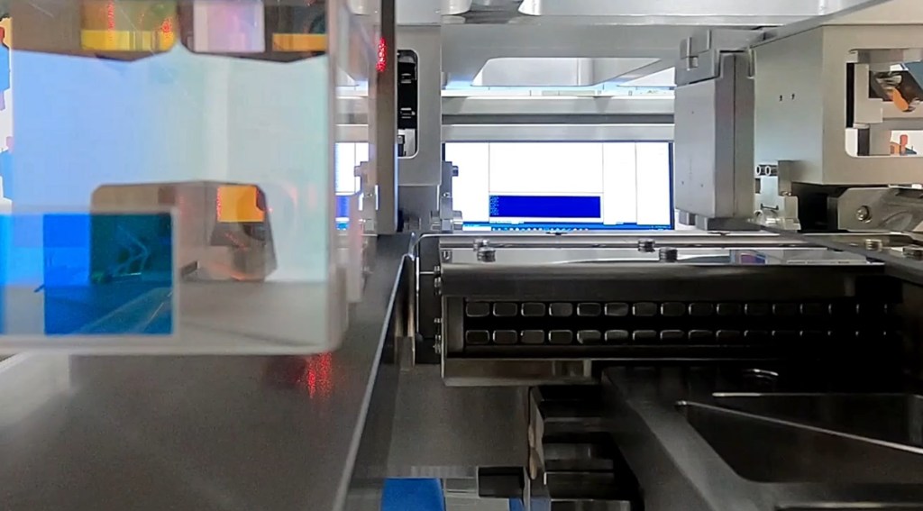
Their new lithography system — essential for printing patterns on chips — is a system built for mass production. The fully automated precision-patterning technology will be used for rapid prototyping, advanced packaging, high-mix production, chip ID, compound semiconductors, and other applications.
The company aims to bring a renaissance to a decades-old technology called lithography, which defines the way a chip designed is printed on a chip. Multibeam’s founders said this is like having the speed of a printing press, or maybe a 3D printer, but with the custom flexibility and adaptability of a pencil.
SkyWater Technology will receive the first system and will use it for early concept prototyping and rapid production of microchips, said David K. Lam, CEO and chairman of Multibeam, and Ken MacWilliams, president of Santa Clara, California-based Multibeam, in an interview with VentureBeat.
Skywater builds both defense and commercial applications in the U.S. Skywater does over a thousand projects a year with Google.
Countdown to VB Transform 2024
Join enterprise leaders in San Francisco from July 9 to 11 for our flagship AI event. Connect with peers, explore the opportunities and challenges of Generative AI, and learn how to integrate AI applications into your industry. Register Now
Lam, one of the pioneers of semiconductor manufacturing, said in our interview that Multibeam could make certain parts of chip fabrication 100 times more productive than current systems. The order from SkyWater is a validation that Multibeam is ready, Lam and MacWilliams said.
“With the push for purpose-built silicon, you get more performance, lower power, and you have better integration. So power is a big factor. All these driving forces, all these unmet needs. And then last but not least, what we’ve changed. We essentially improved the productivity of E-Bea by a factor of over 100,” MacWilliams said. “That was game changing.
It’s all part of a diabolical plan by Lam and his company to keep Moore’s Law going. Named after the late Intel chairman emeritus Gordon Moore, the law held that the number of components on a chip could double every couple of years. It defined tech progress ever since Moore made his prediction in 1965.
Compounded over decades, the advances that come from Moore’s Law have enabled technological progress on a scale the world has never seen. By shrinking atomic dimensions in chips, or miniaturizing them, chip makers have been able to shorten the distance between circuits, enabling electrons to move faster through the chips while the chips consume less material and power. Moore’s Law meant that chips could get faster, cheaper and smaller all at the same time.
But the easier ways of upholding Moore’s Law have stalled. These days, chip makers, designers and equipment makers have teamed together to come up with innovations in 3D packaging, which has resulted in better performance and faster interconnections — but often these chips are much larger than in the past. And many of the latest chip factories can cost $20 billion to build. Those factories cost that much because they’re loaded with precision machinery like those built by Multibeam to process chips.
The early Multibeam team kept the tech alive, but Lam took it over after it started failing. The team got its first chunk of money to build a working prototype around six years ago. The prototyping work proved the tech proof of concept was real. And that led to a production system. MacWilliams said the tech is impressive and it shows that ingenuity continues to burn bright in Silicon Valley.

I asked Lam what has changed in the market, and how thta helped Multibeam stay alive as it developed its technology. Lam said that many folks have predicted the end of Moore’s Law.
“Let’s admit it is over,” Lam said. “The ASML roadmap says at best you’re going to get maybe a factor of 0.7 over the next twelve to 14 years. So the only place to really make a gain is going to be by stitching more chips together. So that puts big pressure on advanced packaging. We have an interesting chart that says, to their credit, Moore’s Law improved transistor density 500 times over the last 20 years. Advanced packaging only did 15 times.”
How it works
Now Multibeam is coming along to propose something different. Multibeam’s platform revolutionizes e-beam lithography (EBL) with new productivity advantages, while enabling high resolution, fine features, wide field of view, and large depth of focus.
The chief productivity driver is the novel architecture which employs multiple miniature columns that operate individually and in parallel, with an advanced control system directing the beams to achieve maximum accuracy, quality, and speed.
Throughput is more than 100 times greater than conventional EBL systems, making the MB platform the highest productivity high-resolution maskless lithography system on the market. It gives manufacturing leaders a breakthrough solution to enable rapid development of new integrated circuit (IC) designs, faster time to market, and accelerated IC innovation.
The platform was developed by a team of semiconductor equipment and patterning technology experts
led by Lam over the past seven years. It is the first EBL system designed from the ground up for volume production, the first one innovated in Silicon Valley, and built by the first US lithography company to emerge in decades, Lam said.
With the launch, Multibeam becomes the sole domestic U.S. supplier of EBL technology. In an age of geopolitical competition between nations, that’s increasingly important.
“We are thrilled to introduce the MB platform and proud to send our first production system to SkyWater,” said Lam. “The semiconductor industry’s growth continues to be fueled by exciting new applications, with advanced lithography technologies enabling endless innovations. At the same time, there is soaring growth in markets like AI and edge computing, where the enablers include purpose-built silicon and advanced packaging, and the manufacturers’ priorities are rapid cycles of learning and cost-effective, seamless transition to production for faster time to market. For these emerging markets, the MB platform offers a complementary lithography solution and expands the range of lithography options available to IC leaders.”
The launch marks Multibeam’s shift from development stage to producer of high-productivity Multicolumn E-Beam Lithography systems. While EBL is valued for its patterning capabilities, low throughput constrained its capacity to take emerging applications from R&D to production.
To unlock the potential, Multibeam re-innovated EBL leveraging well-established technologies to reduce risk. As the MB platform evolved, new applications were emerging with technical, economic, and time-to-
market imperatives that could be addressed with a non-mask-based lithography solution.
“This dynamic affirmed our conviction that an EBL system, re-engineered for high productivity, could
enable applications at advanced nodes for the first time,” said MacWilliams. “The performance advantages are especially compelling in advanced packaging where our system can enable improvements in chip-to-chip power, along with bandwidth and latency. This is helping to drive a new technology inflection that the industry is starting to call ‘advanced integration’ — where new chip-to-chip interconnects can achieve comparable performance to on-chip interconnects.”
MacWilliams added, “We are proud to enable this inflection with a production-proven lithography solution, and confident that our system will help chipmakers seize profitable new market opportunities.”
EBL: Re-innovated for ultra-high productivity
The team designed the platform from the outset for volume production, and more than 40 patents protect the innovations.
In addition to the multicolumn vector-writing architecture which drives productivity, accuracy, and speed, the platform offers auto wafer loading and alignment from wafer cassette to the exposure process in the system.
“We basically reinvented E-Beam lithography,” Lam said. “We were well aware of the fact that it has been dismissed for decades. It was dismissed as slow. And if I didn’t get laughed out of the room, I would be lucky. However, to the team’s credit, they really made a huge effort in every aspect to develop the capability that (the rival) optical technology cannot do. That really makes the foundation for today’s advanced packaging.”
MacWilliams said that purpose-built silicon helps chip designers get to market quicker. By innovating in the packaging, chip design firms like Nvidia are taking two chips and making them function together inside the same package as if they were one chip. That helps get performance gains.
Uptime is optimized by an automated vacuum recovery system, along with a speedy column replacement process and calibration technology. The advanced automation capabilities reduce operator requirements and further contribute to the system’s cost-of-ownership benefits.
As a mask-less lithography solution, the platform offers additional advantages. Where it can take weeks
to develop optical masks, designs can be written in hours with the MB platform. This gives manufacturers greater IC design latitude, while reducing costs and accelerating time to market.
To further enable design flexibility, the platform leverages technology from EDA leader, Synopsys, to generate write recipes, which lets customers achieve their most intricate patterns. With a powerful
built-in data prep system, developed in conjunction with Synopsys, the system writes the chip layouts
directly onto wafers without masks.
Finally, with a compact footprint the system has lower power requirements and needs less fab space. It
is modular by design, with modules easily added as needed for new applications or even higher throughput. In addition, it is fully self-contained and requires no special environment, which further
reduces costs. The system is available in 150mm, 200mm and 300mm configurations.
Source link